| C L E A N R O O M |
The cleanroom is located in the basement of the laboratory building.
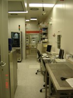
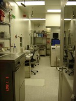
Views into the cleanroom
General data:
- About 120 m² cleanroom, class 1
- Temperature: 20.5 ± 0.5 °C
- Humidity: 42.5 ± 2.5 % (rF)
- Gas system: Purity 6.0 or better) for the most common gases (N2, O2, Ar, H2), the highest purity available for all other gases (CVD, plasma processing) (All data are continuously monitored)
Equipment
The cleanroom is a central service area of the institute. The general process line is for silicon wafers (diameter 3 to 8), but also III/V compounds are handled and processed.
Equipment is installed for the most common processes, such as for
|
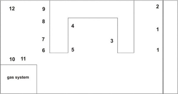
1 2 3 4 5 6 7 8 9 10 11 12 |
 1. cleaning (wet chemical cleaning, dry cleaning),
 2. Photolithography (MA6/BA6),
 3. Special equipment for semiconductor wafer direct bonding including
- CL 200 for direct bonding in an atmospheric environment (or in combination
with MA6/BA6 for aligned wafer bonding)
- NP 12 for plasma-activated wafer bonding using dielectric barrier discharges (DBD)
- SB6 for direct bonding in defined atmospheres or vacuum,
 4. Plasma etching (RIE/ICP) in different fluorine or chlorine ambients (including also
cryo-etching and deep reactive ion etching (DRIE) using the Bosch process),
 5. Plasma-enhanced chemical vapour deposition (PE-CVD),
 6. Low-Pressure chemical vapor deposition (LP-CVD),
 7. annealing processes in hydrogen atmospheres,
 8. Dry cleaning and resist stripping,
 9. Rapid thermal processing (RTP),
 10. Annealing and deposition processes (horizontal furnace) for wafers up to 6 in. in diamete,
 11. Annealing and deposition processes (vertical furnace) for wafers up to 8 in. in diameter,


